**Ultra-Low Jitter 1:6 LVDS Fanout Buffer: ADCLK854BCPZ-REEL7 for High-Speed Data Converters and Synchronization Systems**
In the realm of high-speed digital systems, particularly those employing precision data converters and demanding synchronization schemes, the integrity of the clock signal is paramount. **Jitter, the timing uncertainty of a clock edge, is often the single greatest limiting factor in achieving high signal-to-noise ratios (SNR) and spurious-free dynamic range (SFDR) in analog-to-digital converters (ADCs) and digital-to-analog converters (DACs)**. As system frequencies escalate into the gigahertz range, the challenge of distributing a clean, low-jitter clock to multiple destinations without degradation becomes increasingly difficult. The **ADCLK854BCPZ-REEL7**, a 1:6 differential fanout buffer, is engineered specifically to meet this critical challenge.
This device accepts a single low-voltage differential signaling (LVDS) or LVPECL clock input and distributes it to six identical LVDS output pairs. Its core value proposition lies in its **ultra-low additive phase jitter performance of a mere 28 fs RMS (typical) over the 12 kHz to 20 MHz integration range**. This exceptionally low noise contribution ensures that the pristine quality of a high-performance source clock, such as one from a low-noise oscillator, is preserved as it is fanned out to multiple high-speed data converters (ADCs/DACs) or FPGAs within a system. By minimizing jitter addition, the ADCLK854 directly safeguards the dynamic performance and accuracy of the entire signal chain.

Beyond its stellar jitter specs, the ADCLK854 offers several key features that make it indispensable in complex systems. It supports a wide operating frequency range up to 2.5 GHz, catering to both current and next-generation high-speed designs. The device also provides **excellent channel-to-channel output skew of less than 10 ps**, which is crucial for synchronization systems where precise alignment of multiple clock signals across different PCBs or system modules is required. This is vital in applications like phased-array radar, massive MIMO systems, and high-performance test and measurement equipment where timing coherence across dozens or hundreds of channels is non-negotiable.
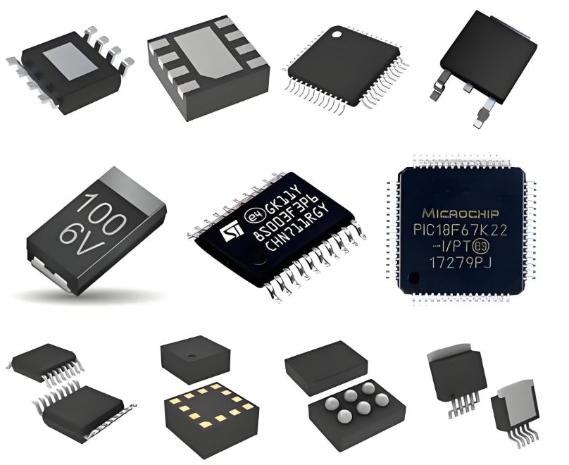
Housed in a compact, 16-lead LFCSP package (3mm x 3mm), the ADCLK854BCPZ-REEL7 is designed for space-constrained environments. Its robust design ensures high reliability and performance stability over temperature and voltage variations. When paired with a high-quality clock source and proper PCB layout techniques—including controlled-impedance differential routing and solid ground planes—this fanout buffer becomes the cornerstone of a high-fidelity clock distribution network.
**ICGOO**
**DFIND Summary: The ADCLK854BCPZ-REEL7 is an ultra-low jitter clock fanout buffer essential for maximizing performance in high-speed data acquisition and synchronization systems. Its core strength lies in preserving clock signal integrity, enabling designers to achieve the highest possible SNR and maintain precise timing alignment across multiple devices.**
**Keywords: Ultra-low jitter, LVDS fanout buffer, High-speed data converters, Clock distribution, Phase synchronization**
